

How To Make A Dc Noise Filter
How to filter out noise in your DC/DC design
After establishing a baseline on power-supply noise, let's focus on mail-filtering strategies of DC/DC converters while driving an analog-to-digital converter (ADC). For continuity with previous posts, I will over again apply the ADC3444, a quad, fourteen-bit, 125MSPS pipeline ADC with low-voltage differential signaling (LVDS) output.
In my "Using a DC/DC converter to power an ADC" mail, I established a baseline using a battery for power followed by 2 unmarried-aqueduct depression-dropout voltage regulators (LDOs) using TI's TPS7A47.The thought hither is to isolate the digital VDD (DVDD) supply of the ADC3444 from the analog VDD (AVDD) supply. Only it's as well possible to achieve the same level of operation of the TPS7A47 reference while using smaller-size, college-efficiency solutions.
The ADC3444 is powered by a TPS54120 DC/DC converter and generates an undesired signal on both the AVDD or DVDD pins that need to be rejected. Figures 1 and 2 illustrate the undesired signals coming from the power supplies. These signals (Figure ane) are originating equally the switching frequency of the DC/DC and are modulated by the ADC clock-phase noise.
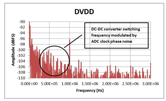
Effigy i: Undesired DVDD signal generated in the power supply
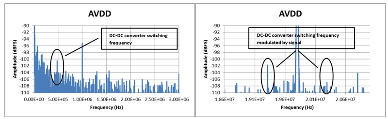
Effigy two: Undesired AVDD betoken generated in the power supply (a) at DC and (b) effectually a single tone
The offset arroyo is to have the signal filtered in the digital domain. To implement this approach successfully, undesirable signals must be deterministic. For DVDD, the undesirable betoken is a modulation of the phase racket with the switching frequency; thus a broad frequency band needs to exist eliminated. For AVDD, the undesirable signal around the unmarried tone, encounter Figure 2, is a lot harder to remove. Thus, digitally filtering this undesirable signal does not seem the best approach. It is therefore critical to remove undesirable signals at their source.
The two options to reduce noise originating in DC/DC converters are π-filters and active devices such as LDOs or power filters.
The π-filter is composed of two capacitors separated past an inductor or ferrite bead. Here, a Murata ferrite bead is selected. The BLM41PG102 has 1kΩ impedance at 100MHz. Figure 3 shows the impedance characteristic.
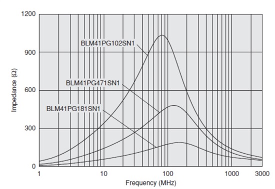
Effigy 3: Murata BLM41PG ferrite-bead impedance versus frequency plot
Looking at the AVDD supply, the ADC3444 has 13 AVDD ability pins, each bypassed by a 0.1µF capacitor. Importing the 0.1µF model from the Kemet library and plotting the π-filter frequency response, y'all have the following curve, encounter Figure 4.
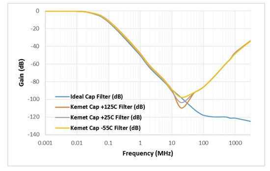
Figure 4: Filter-frequency response for various capacitor temperatures
This filter is essentially behaving as a second-order response with a -3dB point at . Integrating the area beneath the platonic capacitor filter and dividing it past f-3dB gives yous the relationship between the -3dB bandwidth and the equivalent brick-wall filter bandwidth used for noise-power calculations (Effigy five).
This plot only provides variations of the filter noise-power bandwidth (NPBW) and indicates that most of the NPBW is contributed below 1MHz.
Here, for the platonic capacitors.
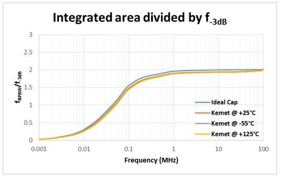
Figure five: Noise-ability bandwidth divided past -3dB bandwidth versus frequency
Now that I've established both the attenuation that the undesirable signals will see prior to reaching the ADC and the constructive NPBW, to aid limit the thermal noise of the power supply, permit's go back to the ADC3444 power-supply rejection ratio (PSRR) on AVDD. The π-filter, made of the BLM41PG102 and thirteen 0.1µF capacitors, improves the PSRR of the ADC by 36dB at 500kHz and will attenuate the thermal racket by an optimistic . (The ratio is optimistic because the largest function of the thermal dissonance is due to noise.) Root mean foursquare (RMS) thermal noise is typically measured over the 10Hz-to-100kHz bandwidth, and the NPBW of the π-filter is 64kHz.
The ferrite bead should be sufficient to eliminate the undesired signals, but information technology is rare to use a 3A DC/DC converter or even a one.2A DC/DC converter solely to operate a 100mA load. If the DC/DC converter was shared by multiple loads, crosstalk betwixt loads would and so get the main problem to resolve.
Let's now plough our attention to agile devices.
LDOs regulate the output voltage to a given accuracy, typically ane to iii per centum. They will accept a high PSRR at DC and decrease as frequency increases. Figure 6 shows the TPS7A81 1A low-noise LDO implemented in an adjustable configuration with the output voltage set by R1 and Rtwo. A feed-forward capacitor (CFeatherbed) is implemented to limit the dissonance and too meliorate the output voltage transient. The noise reduction capacitor (CNR) reduces the noise originating in the on-bit voltage reference. Input and output capacitors are present.
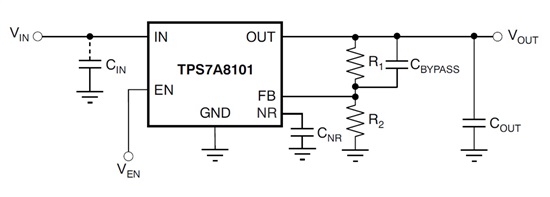
Effigy 6: LDO compages
In contrast, a ability filter regulates the voltage differential between the input and the output. This architecture has no PSRR at DC, and the PSRR increases with frequency. Figure seven shows the TPS7A35 1A low-noise ability filter. Since the voltage drop betwixt input and output is regulated, the voltage drop is set up with a single resistor (RNR). Dissonance reduction (CNR) and the input and output capacitor are present also. This solution can be bonny for its modest PCB footprint.
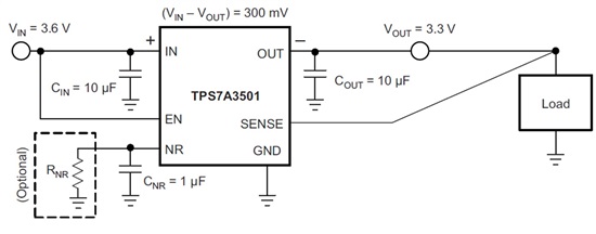
Figure 7: Power filter architecture
Table 1 lists the pros and cons of each solution.
| Category | Ferrite bead | LDO | Power filter |
| PCB area | Big PCB surface area required to minimize internal series resistance | Dependent on LDO selected | Smallest PCB footprint surface area |
| Load transient | Does not provide any regulation. Load transient will become a line transient and lower the load supply voltage. The faster the load transient, the larger the resulting line transient. | Excellent load regulation | Excellent load regulation |
| Noise | Passive filters do not add racket to the organization, merely also do non have any DC rejection | Excellent thermal noise characteristics | Splendid thermal noise characteristics |
| PSRR | Expert rejection, dependent on the concrete characteristic of the ferrite bead and the load ability-supply bypass capacitance | Best DC rejection, independent of load power-supply bypass capacitance. Expect at minimum required output capacitance for stability issues. | No DC rejection, best Air-conditioning rejection |
| Power consumption | None | Linked to dropout voltage | Set dropout |
| Overall | Best for large current (>5A), as there are few other solutions bachelor. Lack of load regulation may be a problem. Tin complement an LDO or power filter. | Best rejection at low frequencies, big component choice | Best Air conditioning rejection, smallest overall solution |
Tabular array 1: Postal service-filtering implementation comparison
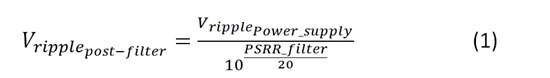
The attenuation provided to the DC/DC ripple by the PSRR for any solution in a higher place will behave as Equation one:
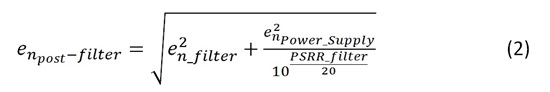
And the thermal noise as Equation two:
In this post, I've looked at various mail service-filtering strategies for the DC/DC converter and adult an belittling approach to compare one solution versus another. In the final installment of this serial, I will put it all together and implement a depression-noise, high-PSRR ability supply and evaluate ADC performance.
In example you missed whatsoever other posts in this series, read my other blogs on creating a power supply for ADCs.

How To Make A Dc Noise Filter,
Source: https://e2e.ti.com/blogs_/b/powerhouse/posts/how-to-filter-out-noise-in-your-dc-dc-design
Posted by: mcbridepootnott.blogspot.com
0 Response to "How To Make A Dc Noise Filter"
Post a Comment